


Key takeaways
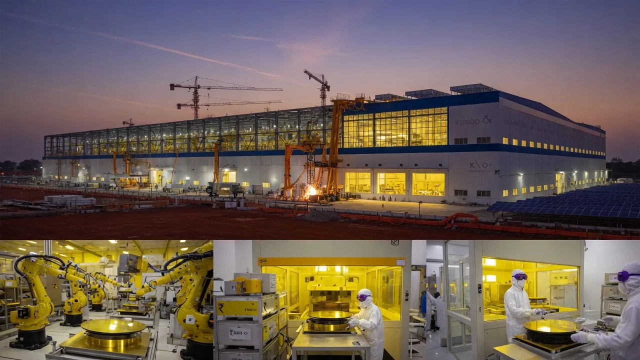
- Applied Materials will invest Rs 3,600 crore in Karnataka after a signed MoU, flagged by minister Patil.
- Money goes into three buckets: R&D, manufacturing of essential semiconductor equipment, and chip software technologies.
- India still imports most high-end wafer tools — this push helps localise critical gear, not just design or assembly.
- Karnataka’s Bengaluru talent pool and design houses make it a natural base for equipment and software work.
- The cheque lands as India scales fabs, OSAT and design under the broader semiconductor mission.
What just happened?
Applied Materials is putting serious money on the table in India.
The US semiconductor equipment maker has signed an MoU for a Rs 3,600 crore investment in Karnataka. Minister Patil flagged the deal after the signed MoU reached his office.
The plan is clear. Research and development. Making essential equipment. Building software the chip industry actually needs.
This is not another vague intent letter. The MoU is signed and received.
For a country still importing most of the high-end tools that etch, deposit and inspect wafers, that matters a lot.
How does this actually work?
Applied Materials sits at the heart of the global chip supply chain. Their tools show up in fabs from Taiwan to the US.
Think of them as the kitchen gear of chip-making. Without the right etchers, deposition systems and inspection kit, a fab does not run clean yield.
Having them build capability here is a different kind of win than just attracting another packaging plant.
The Rs 3,600 crore splits into three practical buckets.
First, R&D. Process labs, materials work, engineering teams that can support local customers and Applied Materials’ global product lines.
Second, manufacturing of essential equipment. Not every chamber or robot will be built in India overnight. But key modules and systems made here cut lead times and grow local supplier networks.
Third, software technologies for semiconductors. Modern fabs run on process control, yield management, scheduling and predictive maintenance software. India already has strong software talent. Pointing that talent at semiconductor-specific stacks is smart.
Rs 3,600 crore is a meaningful cheque. It will not fund a full mega-fab on its own — and it does not need to. Equipment and software sit upstream of wafer starts. Without the tools and the code that runs them, fabs stay hooked on imports and foreign service teams.
Applied Materials has long supplied materials engineering for deposition, etch, metrology and related steps. Their India footprint has historically leaned sales, service and some engineering. Scaling into manufacturing and deeper R&D changes that.
Expect hiring across mechanical, electrical, process, software and supply-chain roles. Expect partnerships with local universities and MSMEs that can machine precision parts or write specialised code.
Timelines and exact site details will firm up as the project moves from MoU to land, clearances and construction. The signal is already public: capital is committed, and the state is treating it as a priority.
What changes for people in India?
India’s semiconductor story so far has focused on fabs, OSAT and design. Tata, Micron and others have announced large projects. Those projects still need tools.
Every new cleanroom that comes online will buy etchers, CVD systems, inspection gear and the software that keeps yield high. If more of that equipment and support can be sourced or serviced from inside India, the whole ecosystem gets cheaper and faster to scale.
Karnataka benefits directly. High-skill jobs. Vendor ecosystems around precision manufacturing. A stronger claim as a semiconductor hub beyond just chip design.
Bengaluru already draws global product companies. Adding equipment R&D and manufacturing gives engineers a reason to stay in process and hardware roles instead of only chasing app or cloud jobs.
For the rest of India the spillover is real. Fab projects in Gujarat, Assam and elsewhere need tool vendors who understand Indian operating conditions — power quality, water, humidity, logistics. A stronger Applied Materials base here helps those sites too.
Localising even parts of the tool-and-software stack reduces risk when geopolitics or shipping lanes get messy.
What should you do now?
If you follow India’s chip push, watch the next steps after the MoU — land, clearances, hiring announcements and which modules actually get made here.
Engineers and students in mechanical, electrical, process, materials and semiconductor software should track openings and university tie-ups. This is not pure assembly-line work.
MSMEs in precision parts, cleanroom components and control electronics can start asking where they fit in the supplier network.
And if you are just a curious phone buyer? You will not feel this in tomorrow’s UPI payment. You will feel it years out, when Indian fabs and packaging lines can stand up faster because more of the “kitchen gear” lives closer to home.





Comments (0)
Be the first to comment!