


Key Takeaways
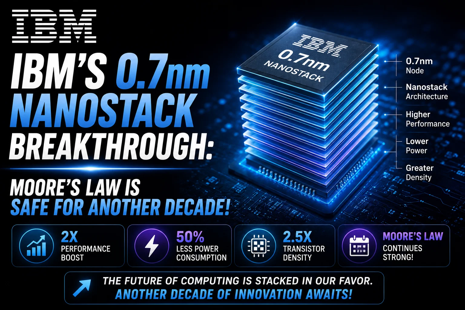
- IBM has successfully detailed a 0.7nm process node, moving beyond the 1nm 'physical limit' previously feared by the industry.
- The new 'nanostack' architecture stacks transistors vertically in 3D, allowing for significantly higher density without increasing the chip's physical footprint.
- This technology is projected to extend the life of Moore's Law for at least another 10 years, ensuring continuous innovation in AI and mobile tech.
- For Indian consumers, this means future devices could see a 200% increase in battery life and massive gains in local AI processing power by the late 2020s.
- The bottom line: IBM isn't just making chips smaller; they are reinventing how they are built to prevent the 'heat wall' that kills modern performance.
The Breakthrough We've Been Waiting For
Remember back in 2021 when IBM shocked the world with the first 2nm chip? Well, it's 2026 now, and while the rest of the industry is just getting comfortable with 1.4nm and 1.1nm mass production, IBM has decided to leapfrog everyone again. They've just detailed a 0.7nm manufacturing process. To give you some perspective, a strand of human DNA is about 2.5nm wide. We are now officially building things at a scale smaller than the building blocks of life itself. This isn't just a minor upgrade; it's a fundamental shift in how we think about computing power and energy efficiency.
For years, critics have been shouting from the rooftops that Moore's Law—the idea that the number of transistors on a chip doubles every two years—is dead. They argued that once we hit the sub-1nm level, quantum tunneling (where electrons just jump across gaps they shouldn't) would make chips useless. IBM's new research says, "Hold my silicon." By using a brand-new "nanostack" 3D transistor architecture, they've found a way to keep the innovation train running for at least another decade. This is huge news for everything from the phone in your pocket to the massive AI servers running the world's economy.
How We Got Here: From FinFET to Nanostack
To understand why 0.7nm is such a big deal, we have to look at how transistors have evolved. For a long time, we used FinFET (Fin Field-Effect Transistors), which looked like little fins sticking up on the chip. Then came GAA (Gate-All-Around) or 'Nanosheets,' which wrapped the gate around the channel for better control. But as we tried to shrink below 1nm, we ran out of horizontal space. You can only pack so many houses on a single plot of land before they start touching and causing problems. IBM’s solution? Build skyscrapers.
The "nanostack" architecture is essentially 3D stacking of transistors at the atomic level. Instead of laying them side-by-side, IBM is stacking N-type and P-type transistors on top of each other. This vertical integration means they can fit twice as many transistors in the same area without making the chip bigger. It also shortens the distance signals have to travel, which reduces latency and, more importantly, cuts down on the heat generated. In 2026, heat is the biggest enemy of performance, and IBM seems to have found the ultimate cooling hack through structural design.
The Nitty-Gritty: Specs and Efficiency Numbers
Let's talk numbers because that's where the real magic happens. IBM claims that this 0.7nm nanostack process can deliver either a 45% performance boost over current 2nm designs or a staggering 75% reduction in power consumption for the same performance level. Imagine your smartphone having the power of a high-end gaming PC from 2024, but the battery lasts for four or five days on a single charge. That is the promise of sub-1nm tech. They are achieving this using High-NA EUV (Extreme Ultraviolet) lithography, which is the most advanced printing process on the planet.
The "nanostack" also utilizes a new type of backside power delivery system. Traditionally, the power lines and data lines on a chip are all tangled up on the top. By moving the power delivery to the back of the wafer, IBM has cleared the "traffic jam" on the front side. This allows for much thicker power rails, which means less voltage drop and better efficiency. It’s like moving the plumbing of a house under the floorboards so you have more room for furniture and people to move around on the main floor. It's a clean, elegant solution to a very messy engineering problem.
What This Means for India
You might be wondering, "This is lab tech in the US, why should I care in India?" Well, India is currently in the middle of a semiconductor revolution. With the India Semiconductor Mission (ISM) in full swing and fabs being built by the likes of Tata and Micron, the global roadmap for chip tech dictates what kind of machinery we buy and what kind of engineers we train. If 0.7nm is the target for 2030-2035, Indian academic institutions and startups need to start pivoting toward 3D architecture design right now.
On the consumer side, this will drastically lower the cost of high-performance computing. As these 0.7nm chips become the standard for servers, the cost of running AI models like ChatGPT or local Indian LLMs will plummet. This means better, faster, and cheaper AI services for every Indian citizen, even on budget devices. We’re looking at a future where a ₹15,000 phone in 2030 could perform real-time, offline language translation with zero lag, thanks to the efficiency of these nanostack transistors.
Real-World Use Cases: Beyond Just Faster Phones
While everyone focuses on phones, the real winners here are Electric Vehicles (EVs) and Edge AI. In an EV, every milliwatt of power saved in the onboard computer translates to more range. A 0.7nm-powered car could potentially manage its battery and autonomous driving systems so efficiently that you get an extra 50-100km of range just from chip efficiency alone. In the medical field, we could see tiny, nanostack-powered sensors that are small enough to be injected into the bloodstream to monitor vitals in real-time without needing a bulky battery.
For the average user, think about Augmented Reality (AR) glasses. The biggest hurdle for AR has always been the weight and the heat—no one wants a hot computer strapped to their face. With 75% less power consumption, 0.7nm chips will finally allow AR glasses to look like normal spectacles while staying cool and lasting all day. We are talking about the end of the "smartphone era" and the beginning of the "ambient computing era," where the tech is invisible but everywhere.
IBM vs The Giants: TSMC, Samsung, and Intel
It's important to note that IBM doesn't mass-produce chips anymore; they develop the "recipe" and then license it to companies like Samsung and Intel. Currently, TSMC is the king of the hill, but their roadmap for 1nm and below has been shrouded in mystery. Intel has been making a huge comeback with their "Intel 18A" and "14A" nodes, but IBM’s nanostack research puts a massive pressure on everyone else to move toward 3D stacking sooner than planned. If Samsung adopts this IBM tech for their 2028-2029 production lines, they could potentially leapfrog TSMC for the first time in a decade.
The competition is fierce because the stakes are trillions of dollars. If you own the 0.7nm process, you own the AI era. TSMC is betting on refined nanosheets, while Intel is betting on RibbonFET and PowerVia. IBM’s nanostack is the most radical of the three, and usually, in the tech world, the most radical design is the one that sets the standard for the next decade. We are seeing a three-way race where the winner will literally dictate the speed of human progress.
TamilTech's Honest Take: Is it Hype or Reality?
Look, we've seen a lot of "lab breakthroughs" that never make it to the factory floor. But IBM has a track record of being right. They predicted the shift to 7nm, 5nm, and 2nm years before they happened. Our take? The 0.7nm nanostack is the real deal, but don't expect it in your iPhone tomorrow. We are looking at a 2029 or 2030 timeline for actual products. However, the fact that the roadmap exists is a huge relief. It means the tech industry isn't going to hit a wall anytime soon.
What we at TamilTech are most excited about is the power efficiency. In a country like India, where heat is a constant factor and charging ports aren't always available on the go, a chip that uses 75% less power is a godsend. We expect this to eventually lead to "forever-on" devices that trickle-charge from ambient light or movement. The next 10 years of chip innovation are going to be wild, and IBM just fired the starting gun for the sub-1nm race. Stay tuned, because the silicon wars are just getting started!






Comments (0)
Be the first to comment!