


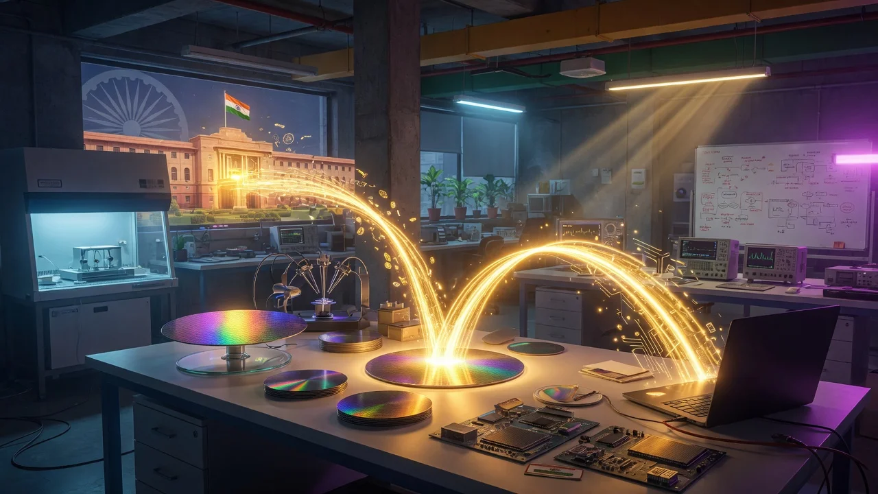
Key takeaways
- Under Semicon 2.0, the government plans to match VC money into Indian chip startups — private capital effectively doubles for eligible deep-tech firms.
- ISM CEO Amitesh Kumar Sinha has flagged this co-investment model as a core pillar for building domestic semiconductor capability.
- Focus is on design, packaging and materials startups that sit beside India's growing fab and ATMP projects.
- Matched funding is meant to de-risk early bets and shorten the road to meaningful chip self-reliance.
- For founders, that could mean more INR flowing into Bangalore, Hyderabad and Noida design houses in 2026 and beyond.
What just happened?
India's semiconductor story just got a sharper funding angle.
Under Semicon 2.0, the government is preparing to match venture capital investments in Indian chip startups. India Semiconductor Mission CEO Amitesh Kumar Sinha has pointed to this co-investment approach as a practical way to pull private money into a sector that still feels high-risk for many VCs.
The idea is simple. When a VC writes a cheque to a qualifying Indian semiconductor startup, the government puts in a matching amount. That instantly doubles the dry powder for hiring talent, buying EDA tools, running silicon spins, or building packaging IP.
This lands at a moment when India already has several large manufacturing and assembly projects moving. What has been thinner is the startup layer that designs chips, creates specialised IP, and fills the gaps between global giants and local demand. Semicon 2.0's matching model tries to fix exactly that gap.
For founders grinding away on RISC-V cores, power-management ICs, or advanced packaging techniques, the signal is clear. The state is willing to sit on the same side of the table as private capital — not only act as a distant subsidy machine.
How does this actually work?
The co-investment model works like a force multiplier.
Venture funds that specialise in deep tech or hardware often hesitate on semiconductor bets. Capital intensity is high. Time-to-revenue looks scary next to a SaaS play. Matching government money lowers that risk.
Put simply: a ₹50 crore VC round can effectively become ₹100 crore of usable capital for the startup. The founder does not necessarily hand the state the same equity stake a private VC would take.
Picture a small chip design house in Bangalore. The team needs EDA licenses, a tape-out, and packaging partner tests. Money runs out fast. A VC round helps, but it is often not enough. When the government match lands, runway stretches. You hire. You buy tools. You run the next silicon spin.
Sinha has framed this as part of a broader Semicon 2.0 architecture that looks beyond the first wave of incentives. Earlier schemes focused heavily on attracting global players to set up fabs and ATMP units. Those remain critical. Semicon 2.0 adds a deliberate startup and design-house layer so India does not end up only assembling chips designed elsewhere.
Eligibility will almost certainly tilt toward companies that are Indian-owned or substantially India-based — working on semiconductor design, compound semiconductors, materials, equipment subsystems, or advanced packaging. Exact rules will firm up with the policy. The direction is already public: match private VC capital to accelerate domestic capability.
On timeline, Sinha has spoken about chip self-reliance as a multi-year journey, not an overnight switch. Manufacturing capacity is coming online in phases. Design talent and IP creation need parallel acceleration. The matching fund is meant to compress that design timeline so that when more fabs are ready, Indian companies actually have products and IP to run on them.
Think of it as building the kitchen and the recipe book at the same time. Fabs are the kitchen. Startups writing RTL, developing chiplets, or creating specialised analog IP are writing the recipes India will eventually own.
Funding will likely flow through existing or expanded ISM mechanisms, possibly alongside SIDBI or other deep-tech vehicles that already understand hardware cycles. The important shift is philosophical: government money now follows private conviction instead of trying to pick every winner alone.
What changes for people in India?
India still imports the overwhelming majority of chips that go into phones, cars, routers, payment devices and industrial machines. Every matched rupee that helps a local design house reach tape-out is a small dent in that import bill and a small gain in strategic autonomy.
Bangalore and Hyderabad already host strong design teams working for global firms. The matching scheme gives more of those engineers a path to build Indian IP, not only ship work abroad. Noida and other clusters can feel the same pull if capital actually lands.
Jobs angle matters too. One mega fab is a huge capital project. Many design and packaging startups growing together create more entry points for engineers, verification specialists and packaging talent. Product companies get a shot at buying local IP instead of waiting on foreign roadmaps.
For VCs, the risk math softens. Hardware cycles stay long. But a matched cheque means the same conviction buys more runway. That is how deep-tech funds that once stuck to SaaS start looking at chip bets again.
None of this makes India self-reliant next quarter. It does make 2026 a year where design houses can raise with less fear that the round dies at the first silicon delay.
What should you do now?
If you are a founder in design, packaging, materials or equipment subsystems, watch the ISM fine print as Semicon 2.0 firms up. Eligibility, match ratios and disbursement routes will decide how usable this really is.
If you are hiring or job-hunting in chip design, keep an eye on Bangalore, Hyderabad and Noida houses that may raise matched rounds. Fresh capital usually shows up first as open roles for EDA, verification and packaging specialists.
If you are an investor, treat this as a signal that the state wants to ride alongside private conviction — not replace it. Diligence still matters. The match only multiplies a bet you already believe in.
And if you are just tracking India's chip story: fabs and ATMP units are the visible half. This co-investment push is the quieter half — the recipe book. Both need to move together.





Comments (0)
Be the first to comment!