


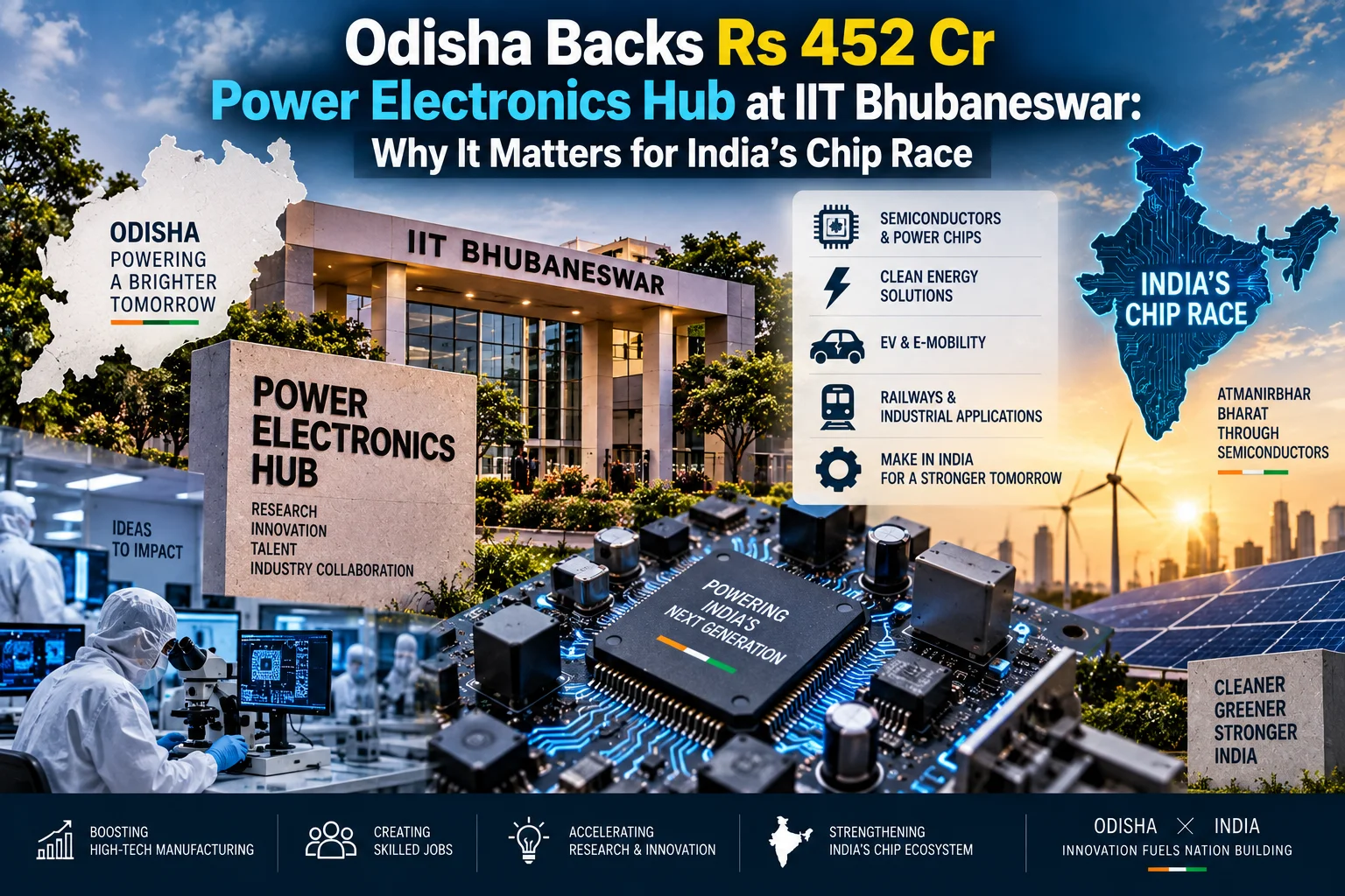
- Odisha approved a ₹452 crore National Industry Co-Development Hub on Integrated Power Electronics at IIT Bhubaneswar.
- Odisha Chief Minister Mohan Charan Majhi shared the update at SEMICON India 2026 in New Delhi.
- The hub targets chip design, advanced semiconductor packaging, and thermal testing under the national semiconductor mission.
- Local hardware makers, EV startups, and solar grid suppliers get direct access to shared industrial testing gear without shipping prototypes abroad.
What just happened in Odisha?
Whenever you see semiconductor headlines, the discussion almost always lands on microscopic 2nm or 3nm processors packed inside flagship smartphones or AI servers. But there is a completely different side of the semiconductor world that quietly controls the physical hardware around us every day: power electronics.
Odisha has stepped into this critical domain by clearing a ₹452 crore National Industry Co-Development Hub on Integrated Power Electronics at IIT Bhubaneswar. Odisha Chief Minister Mohan Charan Majhi announced the project during the SEMICON India 2026 conference in New Delhi. The initiative is being set up under the broader national framework focused on semiconductor design, advanced packaging, and integrated systems.
Instead of building a typical academic laboratory with restricted access, the state and the institute are setting up a shared industrial co-development floor. The idea is straightforward: hardware companies, EV startups, and IIT researchers will work under the same roof to design, package, stress-test, and certify high-power semiconductor systems right here in India.
What are power electronics, and why do they matter?
Think about what takes place every time you plug an 80W fast charger into your smartphone, charge your electric scooter at home, or switch on a 1.5-ton inverter air conditioner. The raw 230V alternating current coming out of your wall socket cannot directly power a lithium battery pack or run a delicate microprocessor. It must be converted, stepped down, filtered, and regulated instantly.
If that conversion fails or leaks excess energy, your phone charger turns into a mini heating iron, or worse, your scooter battery management unit shuts down. Power electronics chips are the high-voltage switches and controllers that handle this conversion quietly inside every modern appliance.
For years, regular silicon chips did this job adequately. But modern hardware demands faster switching speeds and far less heat loss. The entire global tech industry is shifting rapidly toward wide-bandgap materials like Gallium Nitride (GaN) and Silicon Carbide (SiC). These materials can handle blistering voltages, switch on and off millions of times a second, and survive extreme thermal stress without breaking down.
Designing a GaN or SiC power module is not just a software task. You cannot simply write code and order a few sample chips online. You need specialized packaging to drain away intense heat, precision test rigs to run thousands of high-voltage cycles, and cleanroom access to build reliable physical prototypes. For an early-stage Indian hardware startup, buying that equipment outright can easily burn through tens of crores of rupees before selling a single unit.
How will the IIT Bhubaneswar hub work?
The ₹452 crore facility at IIT Bhubaneswar directly addresses this expensive bottleneck. By creating a shared co-development facility, the hub brings high-end thermal design tools, packaging lines, and industrial-grade qualification setups into one shared space.
Hardware founders and tier-1 component suppliers will not have to mail their prototype circuit boards to testing labs in Taiwan, Germany, or the US just to check if a power switch survives thermal runaway. Instead, engineering teams can build their designs, mount them inside advanced packaging, test them under real load conditions alongside IIT faculty and research scholars, and iterate on design flaws within days rather than waiting four months for overseas lab results.
This co-development approach also bridges a long-standing gap in Indian engineering. For decades, university labs published theoretical research papers while private hardware companies struggled to find locally validated components. Putting both groups on the same workshop floor changes that dynamic completely.
How will this impact everyday tech in India?
You might wonder how a research and packaging facility located on the outskirts of Bhubaneswar changes things for an everyday consumer buying gadgets on Flipkart or riding an electric bike to work. The impact will show up across four practical areas over the coming years.
First is electric mobility. Indian roads are a harsh testing ground for electronics. Between 45°C peak summer heat in North India, humid coastal monsoons, and unpredictable bumper-to-bumper traffic, motor controllers take a beating. When domestic EV brands rely on imported off-the-shelf power switches built for mild European weather, motor controllers overheat and cut power. Designing and testing power modules specifically for Indian climate profiles means fewer breakdowns, better range efficiency, and safer battery packs.
Second is renewable energy and local power infrastructure. Solar farms, rooftop solar setups, and battery storage banks need rugged power inverters to feed clean energy into the state power grid without tripping. Developing long-lasting domestic power switches cuts replacement costs and protects our power distribution networks from unexpected hardware failures.
Third is consumer electronics. Those pocket-sized 65W and 100W GaN chargers that used to cost ₹3,000 as expensive imports are becoming everyday accessories. Having domestic design and packaging infrastructure helps Indian accessory brands build reliable, certified power adapters locally at much better price points.
Finally, there is the engineering workforce. India already has deep talent in digital chip design and software simulation. What our engineering ecosystem has lacked is deep practical experience in power packaging, thermal management, and physical semiconductor reliability testing. This hub gives graduate engineers direct hands-on experience with industrial machinery before they step out into the job market.
What should you do next?
If you are an engineering student or researcher working in VLSI, power systems, or material science, track the collaborative research programs and specialized packaging labs opening up at IIT Bhubaneswar. Power semiconductor engineering is turning into one of the most lucrative hardware hiring fields in India as global automotive and electronics suppliers expand their local design teams.
If you run a hardware startup or an EV component brand, reach out to the incubation and industry partnership cells at IIT Bhubaneswar. Getting early access to shared packaging and testing infrastructure can shave months off your product certification timelines and save substantial seed capital.
For everyday tech enthusiasts, this ₹452 crore project is a welcome reminder that building a resilient domestic tech industry requires more than just assembling imported circuit boards. Investing in the underlying power silicon is what truly anchors long-term hardware self-reliance.





Comments (0)
Be the first to comment!